Because it has this:-
instead of having ROM.
At the time the PDP-8 family started out, there were great difficulties with memory. Core memory (RAM) was very expensive and generally very limited. ROM was limited to a very few bytes and usually consisted of a diode matrix. The contents of ROM could be changed by removing diodes with a pair of cutters or soldering in new ones.
When a PDP-8 is first turned on it contains NOTHING, there are no instructions built into the machine to tell it about paper tape readers or teletypes, it is completely empty.
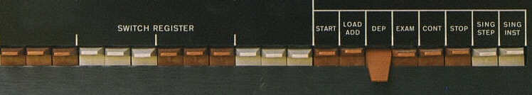
On machines such as this, there has to be some other way of getting instructions in and then starting the execution of those instructions. This is where the programmer's console comes in. The console is mounted on the front of the machine, below the processor & memory. It consists of an array of indicator lights and switches.
The switches on the console from left to right are:-
In addition to the switches there are...
...the indicators, mounted on the panel just above the switches.
The indicators are small incandescent bulbs mounted behind translucent areas of the programmer's console. (Unfortunately, when this photograph was taken, there were no small incandescent bulbs present behind the panel, because their leads had all corroded and they had dropped off. When they are working, the "holes" in the panel light up.)
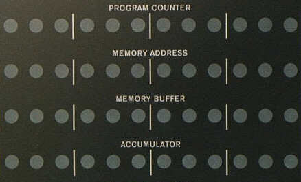
This combination of switches and indicators allows the programmer to enter a program and data, to run or step through the program and to check the working of the program by examining memory locations or the machine's registers.
There is a very simple test program for the PDP-8 which increments the accumulator slowly and this shows as a moving pattern on the Accumulator indicator lights. Remember, the PDP-8 is a 12 bit machine, so the accumulator (or a memory location) can have a value between 0 and 4096. If the accumulator holds 4096 and 1 is added, it then goes round to 0000 again. The program is:-
     Label 1     Increment the Accumulator
     Label 2     Increment a counter, if the counter contains
                    zero, then skip over the next instruction.
                 Jump to Label 2
                 Jump to Label 1
All this program does is add one to the accumulator, then it counts from 0 up to 4096, then it adds another one to the accumulator and so on ... The adding up to 4096 is sufficient delay so that the higher order accumulator lights can be seen to be switching on and off rather than just flickering rapidly.
The PDP-8 program would look like:-
     Address     Content     Instruction
     0020        7001         IAC      Increment the accumulator
     0021        2034         ISZ 24   Increment location 0024, skip next instruction if zero
     0022        5021         JMP .-1  Jump back one place
     0023        5020         JMP .-3  Jump back to beginning
     0024        ????                  The counter
This program would be loaded into the computer as follows:-
     Set 0020 (the start location) on the switch register and depress LOAD ADD key.
     Set 7001 on the switch register and raise the DEP key.
     Set 2034 on the switch register and raise the DEP key.
     Set 5021 on the switch register and raise the DEP key.
     Set 5020 on the switch register and raise the DEP key.
The program is now loaded. Before it can be run, the start address needs to be set.
Set 0020 on the switch register and depress the LOAD ADD key.
Finally
Depress the START key.
The accumulator lights start changing and the program will keep running until the STOP switch is depressed. If the computer is turned off, the program will still be in memory when it is next turned on and may be run again. Core memory doesn't require power to hold its contents.
How do you enter 7001 or 2034 onto 12 switches when the biggest 12 bit number is 4096?
The 12 switches represent 12 binary bits and each can represent either a "1" or a "0" Now, look at the numbers 0 to 10 and their (6 bit) binary and OCTAL equivalents:-
     DECIMAL       BINARY         OCTAL
       00          000 000          00
       01          000 001          01
       02          000 010          02
       03          000 011          03
       04          000 100          04
       05          000 101          05
       06          000 110          06
       07          000 111          07
       08          001 000          10
       09          001 001          11
       10          001 010          12
Two things to notice.
Firstly, there is no direct correspondence between decimal numbers and binary. For instance, 01 decimal is 000�001 binary and 10 decimal is 001�010 binary. The decimal 1s represent 001 in each case but the decimal zero represents 000 or 010. From a decimal number it is possible to calculate the equivalent binary, but the decimal representation does tell us directly what the binary looks like.
But, secondly, if we look at the OCTAL, a "1" always corresponds to "001" and a "0" always corresponds to "000". This is true for all octal numbers. An octal "7" always corresponds to the binary 111, irrespective of its position value. An octal number, therefore, gives a good picture of the appearance of a binary number as well as representing its value.
     0007        000 000 000 111
     0070        000 000 111 000
     0700        000 111 000 000
     etc.
Octal numbers are, therefore, a good shorthand way of writing binary numbers. This is especially true when it is possible to divide the binary into columns of three, ie with 12, 18, 24 or 36 bit machines. DEC used octal to portray the binary for the PDP-8 series and the numbers for the program codes are written in octal. It is not so appropriate to use octal with more modern machines, which tend to be based on multiples of 8 bits (16, 32 & 64bit machines); here the horrible hexadecimal is more suitable.
So going back to the program, the octal numbers in the program represent the following binary numbers:-
             7001         111 000 000 001
             2034         010 000 011 100
             5021         101 000 010 001
             5020         101 000 010 000
It is easy to do the conversion from octal to binary in your head (you only have to remember eight different things and one of those is 0). The control panel switches are coloured in groups of three to help with the conversion.
The pdp-8 has a fairly reduced instruction set. The first three bits of the instruction word specifies the OP-code, so there can only be eight basic instructions.
The PDP-8 handles memory addressing in its own sweet way, (it's almost as weird as the 80x86). Because of the limitation of the word length (12 bits), and the need to use three bits of the word for the instruction code, that leaves only 9 bits for a memory address.
This is not enough.
The PDP design gets round this by dividing memory into 32 pages of 128 words per page. To address the contents of a page then requires 7 bits. This leaves 2 bits. These are used to handle paging and indirect addressing. The indirect addressing uses locations in page zero to hold absolute 12 bit address pointers, and so all memory locations can be accessed.
What follows ignores indirect addressing and just deals with addressing on a single page. This illustrates the principle without the complication.
Just remember, for instructions 0 to 5, three bits hold the instruction, two bits do something else and the last 7 bits of the instruction word contain an address. In the blurb below, this address is referred to as Y.
Instructions 6 and 7 do not address memory and the last 9 bits of their instruction words are defined differently (see the table).
Briefly then, the instructions are:-
| CODE | INSTRUCTION | FUNCTION |
|---|---|---|
| 0... | AND Y |
Logical AND. The content of the memory location Y is bitwise ANDed with the accumulator and the result stored in the accumulator. |
| 1... | TAD Y |
Two's complement add. The content of the memory location Y is combined with the accumulator by two's complement addition. The result is stored in the accumulator. |
| 2... | ISZ Y |
Increment and skip if zero. The content of the memory location Y is incremented by 1 and restored to memory. If the resultant content of Y is now zero the PC is incremented by 1 causing the next instruction to be skipped. Otherwise, the PC is unaltered and the next instruction is executed normally. |
| 3... | DCA Y |
Deposit and Clear the Accumulator The content of the accumulator is stored in memory location Y and the accumulator is set to zero. |
| 4... | JMS Y |
Jump to Subroutine PDP-8 subroutines are handled differently to the way they would be today. The PDP-8 has no stack and no registers in which to store the return address, so the JMS instruction writes the return address into the first word of the subroutine code and starts execution from the second word. To return, a jump is made using the stored return address. |
| 5... | JMP Y |
Jump. Jumps to the address Y |
| 6... | IOT |
Input Output Transfer This instruction handles peripherals. 6 bits of the instruction word specify the device, so up to 64 devices can be addressed directly. The remaining three bits specify the operation to be carried out (7 possibilities) |
| 7... | OPR |
Operate Vaguely named and difficult to describe briefly. There are two groups of operate instructions, depending on the value of bit 4 of the instruction word. The remaining eight bits of either group each correspond to a particular operation, so if a bit is set the action specified for that bit is taken. The beauty of the operate instruction is that if say two bits are set, then one instruction will initiate two actions. Eg, the code 7001 will increment the accumulator. The code 7040 will complement the accumulator. The combination of these codes, namely 7041, will complement and then increment the accumulator. The operate instruction covers a host of different actions, shifting, clearing, complementing, conditional jumps. |